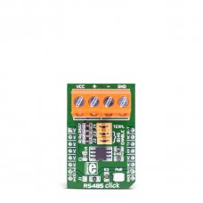
RS485 click 5V
Description
RS485 click 5V carries the ADM485 differential line transceiver from Analog Devices. It is designed for balanced data transmission and complies with EIA standards RS-485 and RS-422. The click is designed to run on a 5V power supply. RS485 5V click communicates with the target microcontroller over UART interface, with additional functionality provided by the PWM pin on the mikroBUS™ line.
ADM485 features
The ADM485 is a differential line transceiver suitable for high-speed bidirectional data communication on multipoint bus transmission lines. It is designed for balanced data transmission and complies with both EIA Standards RS-485 and RS-422. The part contains a differential line driver and a differential line receiver. Both the driver and the receiver may be enabled independently. When disabled, the outputs are tri-stated.
Up to 32 transceivers may be connected simultaneously on a bus, but only one driver should be enabled at any time. It is important, therefore, that the remaining disabled drivers do not load the bus. To ensure this, the ADM485 driver features high output impedance when disabled and also when powered down.
How the click works
There are four screw terminals on the board. Those marked with “+” and “-” are RS485 differential high and differential low communication lines. We added two more terminals for VCC and GND reference if needed for further interfacing. Communication with the board is done using simple UART interface.
Specifications
| Type | RS485 |
| Applications | Board is suitable for Low power RS-485 systems, DTE/DCE interface Packet switching, Local area networks (LNAs), Data concentration, Data multiplexers, Integrated services digital network (ISDN) and more. |
| On-board modules | ADM485 differential line transceiver |
| Key Features | Meets EIA RS-485 standard; 5 Mbps data rate; Short-circuit protection |
| Key Benefits | Superior upgrade for LTC485 |
| Interface | UART,GPIO |
| Input Voltage | 5V,5V |
| Compatibility | mikroBUS |
| Click board size | M (42.9 x 25.4 mm) |
Pinout diagram
This table shows how the pinout on RS485 click 5V corresponds to the pinout on the mikroBUS™ socket (the latter shown in the two middle columns).
Jumpers and settings
| Designator | Name | Default Position | Default Option | Description |
|---|---|---|---|---|
| J1 | PWR. SEL. | Right | 5V | Do not touch, not selectable by user |
| J2 | Bias Enable | ON | ||
| J3 | Bias Enable | ON | ||
| J4 | Term. | ON |
If the board is the first node of the RS485 network, all three jumpers J2-J4 should be placed. If the board is a node in the middle, all jumpers should be removed. If the board is the last node of the RS485 network, place only J4 termination jumper.
Downloads
LibStock: RS485 click 5V libraryEnter the code in the box below:


