PIXI™ click
Description
PIXI™ click is equipped with MAX11300 IC from Maxim Integrated, which features Maxim Integrated's versatile, proprietary PIXI™ technology - it is the industry's first configurable 20-channel mixed-signal data converter. Besides the 12bit multichannel SAR ADC and buffered DAC, it also features one internal and two external temperature sensors for tracking the junction and the environmental temperatures. Adjacent pairs of ports can be configured as logic-level translators for open-drain devices or analog switches. Each port is individually configurable with up to four selectable voltage ranges within -10 V to +10 V.
PIXI™ ports provide highly flexible hardware configuration for 12-bit mixed-signal applications. The MAX11300 is best suited for applications that demand a mixture of several analog and digital functions, such as monitoring and adjusting the bias on the power amplifiers, digital level shifters, automatic fan speed controllers, etc. Actually, it can easily adapt to specific application requirements, allowing for an easy reconfiguration, which makes it usable in virtually any embedded application.
How does it work?
The main component of PIXI™ click is the MAX11300 integrated circuit. The main feature of this IC is the proprietary PIXI™ technology. PIXI™ is an abbreviation for the Programmable mIXed signal In/Out, a technology that allows very flexible routing of both digital and analog signals. The MAX11300 IC has 20 configurable mixed-signal I/O ports. Each port can be independently configured as a DAC output, an ADC input, a GPI, a GPO, or an analog switch terminal. User-controllable parameters are available for each of those configurations. The device also features one internal and two external temperature sensors with the ±1˚C accuracy. The device uses the SPI Mode 0 interface for the communication with the controller, with the clock up to 20MHz.

Analog to Digital Converter
The MAX11300 device features a12bit successive approximation (SAR) ADC module, which can sample signals on a single port up to 400Ksmp/S. Like all the segments of this device, it also offers great flexibility; the signal can be both unipolar or bipolar. Each ADC-configured port can be programmed for one of four input voltage ranges: 0V to +10V, -5V to +5V, -10V to 0V, and 0V to +2.5V. There are two inputs for the reference voltage, but also internal reference voltage of 2.5V can be used, instead.
The converter can be triggered by the CNVT# pin, routed to the PWM pin of the mikroBUS™. This pin has to stay in the LOW logic state for at least 0.5 µs to trigger the conversion. There are several modes of conversion, which include sampling on a single port, or sweeping through all the configured ADC ports.
ADC offers the averaging feature, too. It can average readings of the ADC-configured ports to blocks of 2, 4, 8, 16, 32, 64, or 128 conversion results.
Digital to Analog Converter
The buffered DAC converter is also 12bit, which can output up to 25Ksmp/s on a single port. The output stage of the DAC is equipped with the driver, which offers ±10V on output and high current capability, by using the dedicated power supplies (AVDDIO, AVSSIO pins of the PIXI™ header). The DAC module also uses internal or external reference voltage. The flexibility of the PIXI™ routing also allows monitoring of the DAC configured ports by utilizing the ADC module. All the DAC ports are protected from overcurrent and such events can generate an interrupt on the INT pin, routed to the INT# pin on the mikroBUS™.
General-Purpose Inputs and Outputs (GPIO)
Each of the PIXI™ ports can be configured either to be the general purpose input or general purpose output pin (GPI/GPO).
When set as the GPI pin, the programmable threshold can be set by its data register, from 0 up to the AVDD voltage. The events like rising edges, falling edges or both can be sensed this way, generating an interrupt.
A GPO pin can have a programmed HIGH logic level, up to four times of the DAC referent voltage. The host can set the logic state of GPO-configured ports through the corresponding GPO data registers.
By combining GPI and GPO configured ports, unidirectional and bidirectional level translator paths can be formed, allowing all kinds of level shifters to be built. Bidirectional level translators are built using adjacent pairs of pins and are meant to work as the open drain drivers, so the pull-up resistors should be used to achieve proper voltage levels.
Analog Switch Operation Mode
Two adjacent PIXI™ ports can form an analog switch with the internal resistance of 60Ω, which is controlled in two ways:
- The signal flow through the two adjacent ports can be controlled by any other GPI PIXI™ port, that is used as the switch.
- The internal switching PIXI™ port is programmed to be permanent ON until that port is set to a high-impedance mode by the host controller.
Temperature sensors
The MAX11300 device also features two external sensors and one internal sensor, covering the range from -40°C to +150°C with a good accuracy of ±1˚C. The external sensor can be a simple diode-connected NPN transistor such as 2N3904, which can be used to measure the die temperature of some other integrated circuits. The MAX11300 device also features the parasitic resistance cancellation mode, for the connected temperature sensing element. Temperature can be read from the temperature registers, with the 0.125°C per LSB value.
Other features
There are several other useful features on the MAX11300 device, such as the advanced interrupt management that triggers an interrupt for many various events. Interrupts can also be masked, allowing only the desired interrupts to affect the INT pin state of the click.
The separate pins for the analog GND and digital GND contribute to the signal quality, especially when it comes to mixed-signal applications, where analog signal paths can easily be influenced by the digital signal interferences. Features such as the Burst Transaction Address Incrementing Modes, simplify the firmware development. While using the simple address incrementing mode, the initial register address pointer will keep incrementing automatically after each read/write cycle, as long as the device stays asserted by the CS pin and the serial clock keeps running. The contextual incrementing mode works similar to the previous mode, with the added ability to loop back to the initial start address, after one group of registers has been cycled through. The contextual incrementing mode works only for DAC and ADC configured port registers. For more information about the registers, please refer to the datasheet of the MAX11300.
Specifications
| Type | ADC,DAC |
| Applications | Best suited for applications that demand a mixture of several analog and digital functions, such as monitoring and adjusting the bias on the power amplifiers, digital level shifters, automatic fan speed controllers, etc. |
| On-board modules | Maxim Integrated MAX11300 |
| Key Features | Maxim Integrated proprietary PIXI™ technology featuring versatile routing of all of the 20 PIXI™ ports, allowing realization of many different mixed signal applications with a single IC, wide range of input and output voltages, both bipolar and unipolar. |
| Interface | GPIO,SPI |
| Input Voltage | 3.3V or 5V |
| Click board size | L (57.15 x 25.4 mm) |
Pinout diagram
This table shows how the pinout on PIXI™ click corresponds to the pinout on the mikroBUS™ socket (the latter shown in the two middle columns).
PIXI™ click electrical specifications
| Description | Min | Typ | Max | Unit |
|---|---|---|---|---|
| Analog power supply voltage (AVDD) | 4.75 | 5 | 5.25 | V |
| Digital power supply voltage (DVDD) | 2.50 | 3.3 | 5.50 | V |
| External supply positive voltage AVDDIO | AVDD | 15.75 | V | |
| External supply negative voltage AVSSIO | -12 | 0 | V | |
| External supply AVDDIO to AVSSIO | AVDD | 24 | V |
Note: For the correct setting of the AVDDIO and AVSSIO voltages, please refer to the MAX11300 datasheet
Onboard settings and indicators
| Label | Name | Default | Description |
|---|---|---|---|
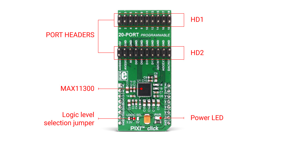
| LD1 | PWR | - |
Power LED indicator |
| HD1 | Port header | - | 20 pin PIXI™ ports connection |
| HD2 | Port header | - | External power, diode temp sensors, analog, references, +5V on board and common GND connection pins |
| JP1 | Logic Sel | Left | Logic voltage level selection, left position 3V3, right position 5V |
Software Support
We provide a library for PIXI™ click on our LibStock page, as well as a demo application (example), developed using MikroElektronika compilers. The demo can run on all the main MikroElektronika development boards.
Library Description
Key functions
void pixi_writeRegister(uint8_t registerAddress , uint16_t registerData) - Generic function for writing to registers.
uint16_t pixi_readRegister(uint8_t registerAddress)- Generic function for reading from registers.
Examples Description
Simple example of LED blinking off all PIXI™ click pins, ports are configured by writing messages to the appropriate registers via the SPI interface. The low-level communication is taken care of inside the MikroElektronika functions. Registers can be easily accessed with two simple functions:
pixi_writeRegister is the register writing function, which accepts two parameters. The first parameter of the function is the 8bit register that needs to be written, while the second parameter is the 16bit data that is written to the register provided with the first parameter. This function does not return any value
pixi_readRegister is used to read the content of a certain register, which is forwarded as an 8bit parameter. This function returns 16bit data which represents the contents of the register, forwarded as the parameter.
The simple application example periodically sets all the GPIO pins to 5V and then to 0V, with one second delay. More information about the registers and their functions can be found in the MAX11300 datasheet.
void applicationTask()
{
    pixi_writeRegister(0x0D, 0xFFFF); //setting all GPIO to 5V
    pixi_writeRegister(0x0E, 0x000F);
    Delay_ms(1000);
    pixi_writeRegister(0x0D, 0x0000); //setting all GPIO to 0V
    pixi_writeRegister(0x0E, 0x0000);
    Delay_ms(1000);
}
The full application code, and ready to use projects can be found on our LibStock page.
Other mikroE Libraries used in the example:
- SPI
Additional notes and information
Depending on the development board you are using, you may need USB UART click, USB UART 2 click or RS232 click to connect to your PC, for development systems with no UART to USB interface available on the board. The terminal available in all MikroElektronika compilers, or any other terminal application of your choice, can be used to read the message.
mikroSDK
This click board is supported with mikroSDK, the MikroElektronika Software Development Kit. To download mikroSDK visit LibStock. For more information about SDK, visit the official page.
Downloads
mikroBUS™ standard specificationsEnter the code in the box below:


