Buck-Boost click
Buck-Boost click™ features LTC3129-1, a buck-boost DC/DC conversion integrated circuit from Linear Technology®. The click supports a wide input voltage range and can output eight discrete regulated output voltage levels, selectable by the digital output voltage selection pins, ranging from 2.5V to 15V.
The main features of this converter are its very low noise and low ripple at the output, as well as very high regulating efficiency and low quiescent current. A proprietary switch control algorithm allows the buck-boost converter to maintain output voltage regulation with input voltages that are above, below or equal to the output voltage. Transitions between the step-up or step-down operating modes are seamless and free of transients and sub-harmonic switching. Manufacturing quality and the design of the Buck-Boost click PCB, ensures that the electrical characteristics are kept within the specs.
Those features make the Buck-Boost click a perfect solution for the regulators and post-regulators for harvested energy, solar panel post-regulators/chargers, rechargeable battery output voltage regulators, wireless low noise applications and similar.
How the click works
The active component of this click board™ is LTC3129-1, a buck-boost DC/DC conversion integrated circuit from Linear Technology®. The LTC3129-1 uses an ultra-low noise 1.2MHz PWM switching architecture, that minimizes the solution footprint by allowing for the low profile inductors and ceramic capacitors to be used.

Buck-Boost click is able to work in two different modes of operation, depending on the nature of the application it is used in - PWM mode and Burst mode.
When the PWM mode is selected, LTC3129-1 operates in a fixed 1.2MHz PWM mode, using an internally compensated average current mode control loop. In PWM mode, ripple and the noise level of the output voltage are minimal.This mode can be selected by setting the PWM pin to logic high level (e.g. connected to VCC). The PWM mode is suitable for working with higher loads connected to the converter output and when the extremely low output noise is required.
For high-efficiency operation at light loads, automatic Burst Mode operation can be selected, reducing the quiescent current down to 1.3µA. Burst mode can be selected if the PWM pin is set to a logic low level (e.g. connected to GND). If the connected load is light enough, the converter will remain working in burst mode, running only when necessary to maintain voltage regulation. Otherwise, the PWM mode will be automatically engaged, providing enough current for the connected heavier load.
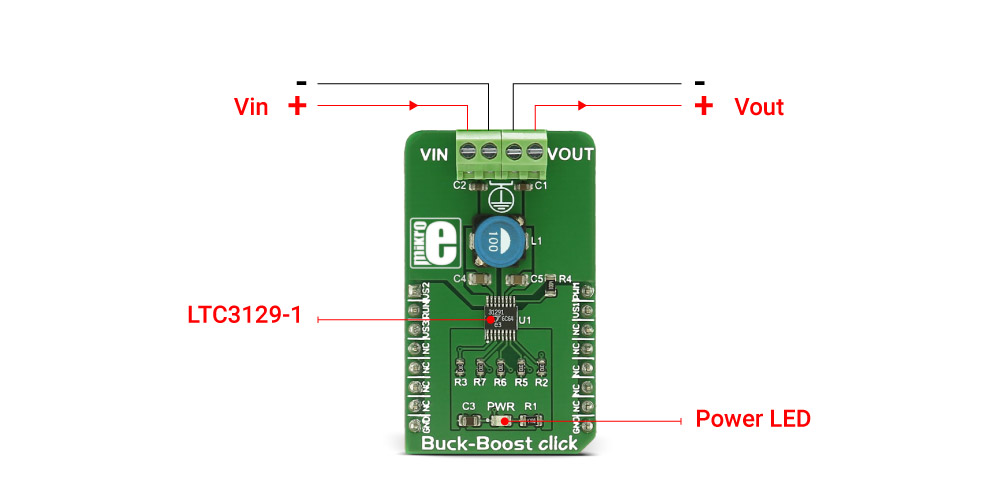
The Buck-boost click powers itself completely from the VIN terminal. Once the power is applied to the VIN terminal, the circuit also has to be enabled by setting the RUN pin to a high logic level. This will power up the converter, which will be indicated by the PWR LED.
The RUN pin function can be utilized to prolong the battery life - for example - the converter can be turned off, preventing draining of the LiPo battery below a certain voltage.
Selection of the desired output voltage is done by setting the output voltage selection pins, as in the table below:
Voltage selection pins settings
| VS3 / CS | VS2 / AN | VS1 / INT | VOUT |
|---|---|---|---|
| 0 | 0 | 0 | 2.5V |
| 0 | 0 | 1 | 3.3V |
| 0 | 1 | 0 | 4.1V |
| 0 | 1 | 1 | 5.0V |
| 1 | 0 | 0 | 6.9V |
| 1 | 0 | 1 | 8.2V |
| 1 | 1 | 0 | 12V |
| 1 | 1 | 1 | 15V |
Specifications
| Type | Boost,Buck |
| Applications | Regulators and post-regulators for harvested energy, solar panel post-regulators/chargers, rechargeable battery output voltage regulators, wireless low noise applications, etc. |
| On-board modules | LTC3129-1 |
| Key Features | Low noise and ripple on the output voltage, high efficiency, wide range of input voltages, selectable stabilized voltage values on the output |
| Interface | Analog,GPIO |
| Click board size | M (42.9 x 25.4 mm) |
Pinout diagram
This table shows how the pinout on Buck-Boost click corresponds to the pinout on the mikroBUS™ socket (the latter shown in the two middle columns).
Buck-Boost click electrical specifications
| Description | Min | Typ | Max | Unit |
|---|---|---|---|---|
| Input voltage range (VIN) | 1.92 | 15 | V | |
| Output voltage range (VOUT) | 2.425 | 15.50 | V | |
| Quiescent current | 1.3 | 1.9 | 3 | µA |
| Inductor average current limit | 80 | 200 | 350 | mA |
Onboard settings and indicators
| Label | Name | Default | Description |
|---|---|---|---|
| PWR | Power LED | - | Power LED indicates that the click is powered on |
| TB1 | VIN | - | Input voltage connector |
| TB2 | VOUT | - | Output voltage connector |
Software support
We provide a library for the Buck-Boost Click on our LibStock page, as well as a demo application (example), developed using MikroElektronika compilers. The demo can run on all the main MikroElektronika development boards.
Library provides the functions that set the voltage level. You can choose between 8 available voltage levels, from 2.5V to 15V.
Key functions
void buckboost_set_2500mV() - Sets Vout to 2.5V
void buckboost_set_2300mV() - Sets Vout to 3.3V
void buckboost_set_4100mV() - Sets Vout to 4.1V
void buckboost_set_5000mV() - Sets Vout to 5.0V
void buckboost_set_6900mV() - Sets Vout to 6.9V
void buckboost_set_8200mV() - Sets Vout to 8.2V
void buckboost_set_12000mV() - Sets Vout to 12.0V
void buckboost_set_15000mV() - Sets Vout to 15.0V
Examples description
The application is composed of three sections:
- System initialization - GPIO initialization
- Application initialization - Sends HAL pointers and initializes the click
- Application task - Cycling VOUT through all of the available voltage levels, in 3 seconds steps.
void applicationTask()
{

    buckboost_set_2500mV();
    Delay_ms(3000);
    buckboost_set_3300mV();
    Delay_ms(3000);
    buckboost_set_4100mV();
    Delay_ms(3000);
    buckboost_set_5000mV();
    Delay_ms(3000);
    buckboost_set_6900mV();
    Delay_ms(3000);
    buckboost_set_8200mV();
    Delay_ms(3000);
    buckboost_set_12000mV();
    Delay_ms(3000);
    buckboost_set_15000mV();
    Delay_ms(3000);

}
Downloads
mikroBUS™ Standard specificationEnter the code in the box below:


