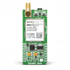
GSM2 click
GSM2 click is the simplest way to add GSM/GPRS communication layer to your project, for fast transmission of data, voice, and SMS. It features the Quectel quad-band M95 FA GSM/GPRS module that has an integrated TCP/IP protocol stack, serial multiplexer and enhanced AT commands. The board contains a quadrupole audio/microphone jack, an SMA antenna connector, as well as a SIM card socket.
GSM2 click is designed to run on either 3.3V or 5V power supply and communicates with the MCU over UART and the following pins on the mikroBUS™ line: INT, PWM, CS, RST and AN.
Note: the antenna is sold separately.
Quad-band frequencies
The M95 FA supports quad-band frequencies — GSM850MHz, GSM900MHz, DCS1800MHz or PCS1900MHz. The module can search these frequency bands automatically.
GPRS data transfer
The GPRS data uplink and downlink transfer is 85.6 kbps, which is high enough for multimedia messaging.
Power consumption
The power consumption of the M95 FA is really low — 1.3 mA in sleep mode.
For more information about the power consumption, see the module’s datasheet.
SMD jumper
There is one zero-ohm SMD jumper J1 used to select whether 3.3V (default) or 5V I/O voltage level is used. Note that, regardless of the logic level, the module requires a 5V power supply in both cases.
Key features
- M95 FA from Quectel
- Quad-band frequency
- 85.6 kbps GPRS data transfer
- Power consumption: 1.3 mA in sleep mode
- On-board SMA connector
- SIM card socket integrated at the bottom side of the board
- 3.5mm quadrupole earphone/microphone jack
- UART interface
- 3.3V or 5V power supply
Specification
| Type | GSM |
| Applications | GSM Click™ with it’s Quectel M95 FA GSM/GPRS module is ideal for mobile devices |
| On-board modules | Quectel M95 FA GSM/GPRS |
| Key Features | GENERAL: Quad-band 850, 900, 1800, 1900MHz. DATA: supports PPP/ TCP/ UDP/ HTTP/ FTP/ SMTP/ SSL protocol stacks with Max. 85.6kbps (uplink & downlink). |
| Key Benefits | SIM card socket integrated at the bottom side of the board |
| Interface | GPIO,UART |
| Input Voltage | 3.3V or 5V |
| Compatibility | mikroBUS |
| Click board size | L (57.15 x 25.4 mm) |
Pinout diagram
This table shows how the pinout on GSM2 click corresponds to the pinout on the mikroBUS™ socket (the latter shown in the two middle columns).
Programming
Code examples for GSM2 click, written for MikroElektronika hardware and compilers are available on Libstock.
The library for GSM 2 click uses the AT parser is to analyze the responses from the module. Depending on the analyzed string, the execution of a user-defined callback function can be implemented for unique user-specific requirements. The following code snippet shows how the GSM engine is initialized. The function calls the initialization of AT adapter, timer and parser. This should be done before executing any other function.
 1 void gsm_engine_init( at_cmd_cb default_callback )
 2 {
 3     at_adapter_init();
 4     at_timer_init();
 5     at_parser_init();
 6
 7     at_cmd_save( "+CMS ERROR :", DEFAULT_TIMEOUT, default_callback,
 8                                                   default_callback,
 9                                                   default_callback,
10                                                   default_callback );
11
12     exception_f = false;
13     response_f  = false;
14     cue_f       = false;
15
16     cb_default = default_callback;
17
18     memset( ( void* )tx_buffer, 0, AT_TRANSFER_SIZE );
19 }
Downloads
mikroBUS™ Standard specification
Enter the code in the box below:


