Flash 4 click
The S25FL512S module can withstand up to 100,000 program cycles, with the data retention period of minimum 20 years. The flash memory IC used on this Click board™ features Serial Flash Discoverable Parameters (SFDP) mode, used to retrieve the advanced information from the device, such as the operating characteristics, structure and vendor specified information, memory size, operating voltage, timing information, and more.
Featuring both normal and double data rates over the standard, Dual/Quad SPI interface, the improved reliability of the stored information by utilizing the hardware Error Correction Code (ECC) generation, One-Time Programmable (OTP) memory block of 1024 bytes, an advanced sector protection, AutoBoot, and much more, this Click board™ is a perfect solution for the mass storage option in various embedded applications. Due to its fast performance, Flash 4 click can also be used for the code shadowing, execute-in-place (XIP), and data storage. An additional level translator IC allows Flash 4 click to be used with a wide range of MCUs, operating both with 3.3V or 5V logic levels.
How does it work?
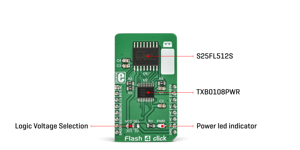
The Flash memory module used on this Click board™ is the S25FL512S, a 512 Mbit SPI Flash memory module, from Cypress. The Flash memory density is usually expressed in bits, so 512 Mbit of memory aligned in 8 bits long words, translates to a capacity of 64 megabytes (MB). This memory module contains 256 sectors of 256 KB each. Furthermore, the memory is organized in 256KB sectors that alow user to erase whole sector only and write up to 512byte at a time.

The advanced MirrorBit® technology allows storing of two data bits in each memory array transistor (memory cell), effectively doubling the capacity of a single storage cell this way. The Eclipse™ architecture is responsible for the greatly improved erase and programming performance, compared to other Flash modules of the previous generation. Due to a higher speed, an execute-in-place (XIP), as well as the data shadowing is possible with the Flash 4 click.
The S25FL512S flash module supports the standard SPI interface, but it can also optionally use the Dual and Quad SPI interface, allowing the full data transfer rate of 80MB/sec to be achieved. In addition, the flash module supports DDR read commands in all SPI modes, using both clock edges to transfer the data (data transfer is performed on both the rising and the falling edge of the clock). A typical communication procedure consists of sending a proper instruction (command) from the host MCU via the SPI interface, followed by either an address, data, or both, and a response from the S25FL512S flash module, which can be either a stream of data or a single byte, depending on the command received.
One of the key features of the S25FL512S is certainly the AutoBoot feature. It allows the module to automatically initiate the memory transfer from the predefined location (memory read operation) after the reset cycle. Considering a typical communication scenario, where READ command followed by the one or more address bytes need be used, AutoBoot allows the host MCU to pull down the #CS (Chip Select) pin and start receiving a data stream over the SPI interface for as long as the #CS pin is held LOW, without any wasted cycles. As soon as the #CS pin is released, the S25FL512S returns to a normal operation.
The Advanced Sector Protection (ASP) is a powerful protection model that incorporates a set of various software and hardware methods to enable or disable programming or erase operations within a sector or an entire memory. A specialized ASP OTP register offers a password protection mode or a persistent protection mode, allowing an increased flexibility of the protection. Using the OTP memory allows the protection mode to remain in place for the whole life-cycle of the device.
The #WP write protect pin is used to put the device into the hardware write protect mode. A LOW logic level on this pin prohibits write operations to the Block-Protection bits of the Status register. Locking down the Status Register will block changes of the Status Register Write Disable (SRWD) bit, which is required for the Write and Erase operations, effectively preventing the memory content changes. The pin is multiplexed with the IO2 function, therefore it is not available when Quad SPI is used
The #HOLD pin is used to hold the data transfer. When the Chip Select pin (#CS, routed to the mikroBUS™ CS pin) is set to a LOW logic level, the data transfer will be put on hold when the LOW logic level of the serial clock coincides with the falling edge of the #HOLD pin. Similarly, resuming the data transfer will happen when the LOW logic level of the serial clock coincides with the rising edge of the #HOLD pin. The pin is multiplexed with the IO3 function, therefore it is not available when Quad SPI is used
The SPI interface pins are routed to the mikroBUS™ so that the interfacing with the microcontroller unit (MCU) is easy and straightforward. Additional pins routed to the mikroBUS™ include the #WP/IO2 pin routed to the mikroBUS™ PWM pin and labeled as IO2, and #HOLD/IO3 pin routed to the mikroBUS™ INT pin and labeled as IO3. There is also the RESET pin, routed to the RST pin of the mikroBUS™, which performs a reset of the Flash module, initiating an AutoBoot sequence if enabled.
There is 1 KB of OTP memory, which can be used to store security data, such as the unique serial number, and similar information. Some security-related registers, such as the password for the ASP, registers for selecting the ASP mode, and similar, are in this memory block. Once programmed, this memory can be permanently locked, without the possibility to reprogram it ever again.
Flash 4 click incorporates an additional IC, labeled as the TXB0108PWR, an 8-bit bidirectional voltage level translator with auto-direction sensing, from Texas Instruments. This allows the Click board™ to be used with a much wider range of MCUs since the S25FL512S flash module operates with logic levels up to 3V. At the same time, the TXB0108PWR protects the flash module from the Electrostatic Discharges (ESD) up to ±15 kV, making Flash 4 click a very robust and reliable embedded mass storage solution. An onboard SMD jumper labeled as VCC SEL can be used to configure the logic voltage level.
For the detailed explanation, please consult the included datasheet. However, MikroElektronika provides a library which contains functions that simplify and speed up working with this device. The provided application example demonstrates the functionality of the library functions. It can be used as a reference for a custom project development.
Specifications
| Type | Flash |
| Applications | Mass storage option in multimedia devices, data drives, non-volatile data storage in embedded applications, secure storage, and similar applications that require reliable permanent storage of digital information. |
| On-board modules | S25FL512S, a 512 Mbit SPI Flash memory module, from Cypress |
| Key Features | High durability of 100,000 write cycles, Advanced Sector Protection (ASP), secure OTP memory block, high transfer speed, SFDP mode for easy retrieval of IC-specific information, AutoBoot function for improved startup performance |
| Interface | QSPI,SPI |
| Input Voltage | 3.3V or 5V |
Pinout diagram
This table shows how the pinout on the Flash 4 click corresponds to the pinout on the mikroBUS™ socket (the latter shown in the two middle columns).
Onboard settings and indicators
| Label | Name | Default | Description |
|---|---|---|---|
| LD1 | PWR | - | Power LED indicator |
| JP1 | VCC SEL | Left | Logic voltage level selection: left position 3.3V, right position 5V |
Software support
We provide a library for the Flash 4 Click on our LibStock page , as well as a demo application (example), developed using MikroElektronika compilers. The demo can run on all the main MikroElektronika development boards.
Library Description
The library contains all the necessary functions for working with Flash 4 click.
Key functions:
void flash4_writeCommand(uint8_t cmd)- Functions for write command
void flash4_4ReadFlash(uint8_t *outData, uint32_t addr, uint8_t nData)- Functions for read Flash, with 4 byte address
void flash4_4PageProgram(uint8_t *inData, uint32_t addr, uint8_t nData)- Functions for write data in Flash, with 4 byte address
Examples description
The application is composed of the three sections :
- System Initialization - Initializes SPI Module and sets RST pin and CS pin as OUTPUT
- Application Initialization - Initialization driver init and reset device
- Application Task - (code snippet) - Erases memory at 0x00001234. Writes a message (MikroElektronika) to address 0x00001234. Then reads the data from the address 0x00001234.
void applicationTask()
{
    flash4_writeCommand(_FLASH4_CMD_WRITE_ENABLE_WREN);
    mikrobus_logWrite("--- Erase chip --START--", _LOG_LINE);
    flash4_4sectorErase(0x00001234);
    while(flash4_checkWIP());
    mikrobus_logWrite("--- Erase chip --DONE--", _LOG_LINE);

    flash4_writeCommand(_FLASH4_CMD_WRITE_ENABLE_WREN);
    flash4_4PageProgram(&dataBuffer[0], 0x00001234, 16);
    while(flash4_checkWIP());
    Delay_100ms();

    flash4_4ReadFlash(&readBuffer[0],0x00001234, 16);
    while(flash4_checkWIP());
    mikrobus_logWrite("--- Read buffer : ", _LOG_TEXT);
    mikrobus_logWrite(readBuffer, _LOG_LINE);

    Delay_ms( 7000 );
}
The full application code, and ready to use projects can be found on our LibStock page.
Other mikroE Libraries used in the example:
SPI
Additional notes and information
Depending on the development board you are using, you may need USB UART click, USB UART 2 click or RS232 click to connect to your PC, for development systems with no UART to USB interface available on the board. The terminal available in all MikroElektronika compilers, or any other terminal application of your choice, can be used to read the message.
mikroSDK
This click board is supported with mikroSDK - MikroElektronika Software Development Kit. To ensure proper operation of mikroSDK compliant click board demo applications, mikroSDK should be downloaded from the LibStock and installed for the compiler you are using.
For more information about mikroSDK, visit the official page.
Downloads
mikroBUS™ Standard specificationEnter the code in the box below:


