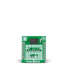
Flash 3 click
The high-performance Flash chip operates at 50MHz at Normal and 133MHz at Fast Read speeds.
It is specified to standard 100,000 erase/program cycles with more than 20 years of data retention. The data can be erased in sectors or blocks and programmed with 1 to 256 bytes per page.
Each chip has a 128-bit unique ID for each device.
Flash 3 communicates with the target board through the mikroBUS™ SPI interface with additional functionality provided by HOLD, CE and WP pins. It is designed to use a 3.3V power supply only.
Specification
| Type | Flash |
| Applications | Mass storage option in multimedia devices, drives, optical and printing devices |
| On-board modules | ISSI IS25LP128 IC |
| Key Features | 128 Mbit capacity, 50/133 MHz read speed (Normal/Fast) |
| Key Benefits | 128-bit unique ID for each device, Software and hardware write protection |
| Interface | GPIO,SPI |
| Input Voltage | 3.3V or 5V |
| Compatibility | mikroBUS |
| Click board size | S (28.6 x 25.4 mm) |
The click board also comes with a firmware library which is very similar to the one used for Flash 2 click, documented in this learn article.
Programming
This example shows the Flash 3 click write routine.
 1 void flash_3_write
 2 (
 3         uint32_t address,
 4         uint8_t *buffer,
 5         uint32_t count
 6 )
 7 {
 8     flash_3_write_enable( true );
 9     flash_3_hal_cs( 0 );
10     flash_3_hal_cmd( FLASH_3_PP );
11     flash_3_write_address( address );
12     flash_3_hal_write( buffer, count );
13     flash_3_hal_cs( 1 );
14     while( flash_3_wip() );
15 }
Code examples that demonstrate the usage of Flash 3 click with MikroElektronika hardware, written for mikroC for ARM, and FT90x are available on Libstock
Downloads
Enter the code in the box below:


