MCP16331 click
MCP16331 click functions as a non-inverting buck-boost voltage regulator, a type of switching mode power supply topology that combines the principles of the Buck converter (step-down) and the Boost converter (step-up) in a single circuit.
The Buck converter produces a DC output in a range from 0V to just less than the input voltage. The Boost converter produces an output voltage ranging from the same voltage as the input to a level much higher than the input.
The MCP16331 click itself produces constant DC voltage on the output rails, which can be set in the code.
A typical application for a buck-boost regulator is a battery-powered system, where the input voltage can vary widely, starting at full charge and gradually decreasing as the battery charge is used up. At full charge, where the battery voltage may be higher than needed by the circuit, a buck regulator would be ideal to keep the supply voltage steady.

Figure 1
However as the charge diminishes the input voltage falls below the level required by the circuit, and either the battery must be discarded or re-charged; at this point, the ideal alternative would be the boost regulator.
By combining these two designs, it is possible to have a regulator circuit that can cope with a wide range of input voltages both higher or lower than that needed by the circuit.
How the MCP16331 click works
The click board(TM) central module is the Microchip's MCP16331, a non-synchronous, step-down or buck converter capable of stepping input voltages ranging from 4.4V to 50V, and output voltage ranging from to 2.0V to 24V. More details about the MCP16331 are available in the official datasheet.
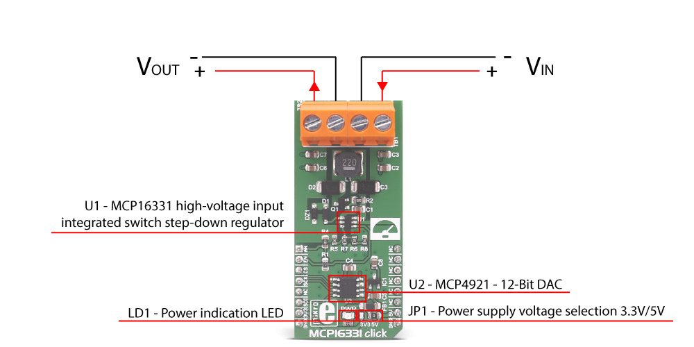
The MCP16331 click is designed to handle an input voltage ranging from 4.5V to 18V and output a voltage ranging from 2,25V to 12V at 500 mA maximum current. The power source is connected to the TB1 (VIN) terminal, and the load is connected to the TB2 (VOUT) terminal, at the top of the click board™ (as you can see in figure 1).
The power circuit is isolated from the logic circuit that, as per the mikroBUS™ standard, can operate at 3.3V or 5V. The voltage is selectable via JP1 switch, by default set at 3.3V, and the green LED (LD1) indicated that this voltage is present.
The MCP16331 click uses the SPI bus present on the mikroBUS™, to communicate with the host processor, however, also uses two extra pins AN and RST that are used respectively for measuring the output voltage and enabling or disabling the MCP16331 output, this is important for the correct power sequence (see note below).
NOTE: To avoid any possible damage to any load connected to the VOUT terminals, you must follow the correct power-up sequence:
- Disable the MCP16331 by setting the mikroBUS™ pin RST (EN) low (GND)
- Set the desired output voltage via SPI (see the software section below)
- Enable the MCP16331 by setting the mikroBUS™ pin RST (EN) high (5V)
The reason for this sequence is that the enable pin (EN) of the MCP16331 has an internal pull-up resistor that keeps the MCP16331 output stage enabled even if the pin is left unconnected.
At power-up, before you set the voltage via SPI, DAC output is unspecified and the output voltage may set higher than what your load supports.
The MCP16331 click gives you the possibility to read the output voltage via analog pin (AN). Using the microcontroller ADC you can read the value, divided by the two 120K and 33K resistors (R1 and R4 on the schematic) that you can calculate with the formula:

So let's suppose that you have set the voltage at 5V:

In this case 1,07V.
This feedback mechanism is useful when you want to set an exact voltage. You can measure the output and adjust the voltage.
Specifications
| Type | Buck |
| On-board modules | MCP16331 high-voltage input integrated switch step-down regulator |
| Interface | SPI |
| Input Voltage | 3.3V or 5V |
| Click board size | L (57.15 x 25.4 mm) |
Pinout diagram
This table shows how the pinout on MCP16331 click corresponds to the pinout on the mikroBUS™ socket (the latter shown in the two middle columns).
MCP16331 click maximum ratings
| Description | Min | Typ | Max | Unit |
|---|---|---|---|---|
| Input Voltage Range (VIN) | 4.5 | 18 | V | |
| Output Voltage Range (VOUT) | 2.25 | 12 | V | |
| Output current | 500 | mA | ||
| Switching Frequency | 500 | kHz | ||
| Efficiency | 96% |
Onboard settings and indicators
| Label | Name | Default | Description |
|---|---|---|---|
| TB1 | VIN | - | Voltage input screw terminal |
| TB2 | VOUT | - | Voltage output screw terminal |
| JP1 | PWR.SEL. | 3.3V | Power supply voltage selection 3V3/5V, left position 3V3, right position 5V |
| LD1 | PWR | - | Power LED, lights green when the power supply is established properly |
Software Support
We provide a library for the MCP16331 click on our LibStock page, as well as a demo application (example), developed using MikroElektronika compilers. The demo application can run on all the main MikroElektronika development boards.
Note: depending on the development board you are using, you may need the RS232 click or USB-UART click or USB UART 2 click, to connect to your PC. The terminal available in all MikroElektronika compilers, or any other terminal application of your choice, can be used to read the message.
Library Description
The library carries a function for controlling the MCP16331 click output alongside with SPI driver initialization function.
Key functions
void mcp16331_setVout(uint16_t millivolt )- Sets voltage on outputs
Examples Description
The application is composed of three sections:
- System Initialization - Initializes GPIO and SPI peripheral, but also and UART used for information logging.
- Application Initialization - Driver initialization.
- Application Task - (code snippet) Periodically changes the output voltage in the range from 5V to 12V. Information about the current output voltage is logged on UART.
void applicationTask()
{
    mcp16331_setVout( 5000 );
    UART1( "rnOutput Voltage changed to 5V" );
    Delay_ms( 3000 );
    mcp16331_setVout( 12000 );
    UART1( "rnOutput Voltage changed to 12V" );
    Delay_ms( 3000 );
}
The example also carries additional functions for GPIO control which are provided during driver initialization. These functions are necessary and implementation depends on development system used.
Other MikroE Libraries used in the example:
- UART
Downloads
mikroBUS™ Standard specificationEnter the code in the box below:


