Boost-INV click
High integration rate of the Boost-INV click allows it to use a low number of external components. Advanced switching control of the LTC3582 allows very high efficiency and reduced EMI for using it in audio, or similar EMI sensitive applications. Output disconnect feature prevents current leaking (battery discharge) when the device is powered off. These features allow this Click board™ to be used as a very compact programmable split-rail power supply used for general purpose applications, low power audio applications, LCD and OLED displays and similar applications that use dual power supply source.
How does it work?
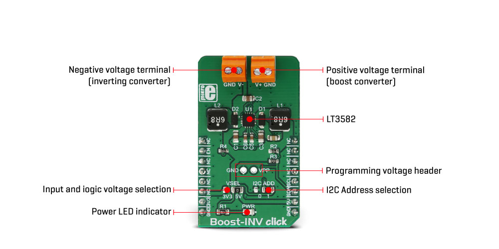
The main component of the Boost-INV click is the LT3582, programmable boost and inverting DC/DC converter with OTP memory, from Analog Devices. This IC is actually a dual circuit, offering a boost DC/DC converter and an inverter, in one package. The boost converter can provide up to 12.78V on the output while driving the load with up to 350mA. The inverter can provide -13.95V, offering up to 600mA to the connected load, before the current limiting is activated.
The boost converter uses an advanced switching scheme with the source-grounded NMOS as the main switching element, controlling both the off-time and the peak current. The programmable voltage divider on the output provides the feedback voltage, needed for the regulation. The inverter topology allows a single inductor to be used on the output, simplifying the design.

As already mentioned, the LT3582 features a set of programmable parameters, which can be accessed via the I2C interface. These parameters include configuring the output voltages, power sequencing, and output voltage ramp rates. An onboard OTP non-volatile memory can be programmed with values that will be used at the startup. The command register (CMDR) is reset to 0x00h upon powering up, which disables the outputs and sets the device to read parameters stored in the OTP area. If the OTP memory area is empty, it is necessary to set up working parameters first (output voltage, power up sequence, charging current for the ramp-up capacitors…), before using the device. It is worth mentioning that there are three bits in the CMDR register, referred to as RSEL0, RSEL1, and RSEL2 in the LT3582 datasheet, which redirects the device to use either registers or the OTP memory. When set to 0, the device uses parameters stored in the OTP memory. Note that 0x00h is the default value of the CMDR register, meaning settings stored in the OTP will be used by default, after power on.
It is possible to dynamically change values of the output voltages and other configurable working parameters. However, it is highly recommended to disable the device (SWOFF bit of the CMDR register) before modifying working parameters, since large output voltage changes can cause large current spikes on the switching circuitry if performed in real-time, while the switching circuit is running.
Programming the OTP requires an external power source, which is fairly filtered (possibly with a filtering capacitor on the output). Voltage drop under 13V might trigger the FAULT bit and render the device unusable. This voltage ranges from 13V to 15V. The Click board™ is equipped with the standard 2.54mm (100mil) header for this purpose. Once the programming voltage is connected (VPP pad), the WOTP bit of the CMDR register initiates the programming. The complete algorithm with the detailed description of the OTP programming procedure can be found in the LT3582datasheet.
An onboard SMD jumper labeled as VSEL allows selection between the 3.3V and 5V power rail from mikroBUS™, routing it to the voltage input pin of the LT3582 IC. The I2C pull-up resistors are also connected to this voltage, allowing communication with both 3.3V and 5V MCUs.
The Click board™ also offers the I2C address selection jumper, labeled as the I2C ADD. This jumper selects between two possible 7bit addresses: left position sets the I2C slave address to 0x49h, while the right position sets the address to 0x69h. Note that this is the 7bit address only - to get the complete I2C address, an R/W bit needs to be added at the end.
Input screw terminals allow secure connection for the load and are clearly labeled to avoid confusion: the V- pin offers the negative voltage, while the V+ pin outputs positive voltage. GND pins are connected to the common ground of the Click board™.
Specifications
| Type | Boost |
| Applications | The Click board™ can be used as a very compact programmable split-rail power supply used for general purpose applications, low power audio applications, LCD and OLED displays and similar applications that use dual power supply source |
| On-board modules | LTC3582, programmable boost and inverting DC/DC converter with OTP memory, from Analog Devices |
| Key Features | Programmable output, OTP memory for storing of default parameters, high efficiency switching scheme, both boosting and inverting options in the same die, low count of external components required, and more |
| Interface | I2C |
| Input Voltage | 3.3V or 5V |
| Click board size | L (57.15 x 25.4 mm) |
Pinout diagram
This table shows how the pinout on Boost-INV click corresponds to the pinout on the mikroBUS™ socket (the latter shown in the two middle columns).
Onboard Jumpers and Settings
| Label | Name | Default | Description |
|---|---|---|---|
| LD1 | PWR | - | Power LED indicator |
| JP1 | VSEL | Right | Input voltage selection: left position 3.3V, right position 5V |
| JP2 | I2C ADD | Right | I2C address selection: left position 0x49h, right position 0x69h |
| TB1 | GND, V- | - | Negative voltage output terminal |
| TB2 | GND, V+ | - | Positive voltage output terminal |
| HD1 | GND, VPP | - | External programming voltage header |
Boost-INV click electrical specifications
| Description | Min | Typ | Max | Unit |
|---|---|---|---|---|
| Input voltage (mounted on the mikroBUS™) | 3.3 | 5 | 5 | V |
| Positive output voltage (boost converter) | 3.52 | - | 12.94 | V |
| Negative output voltage (inverting converter) | -1.18 | - | -14.2 | V |
| Switching current limit on V+ (boost converter) | 285 | 430 | mA | |
| Switching current imit on V- (inverting converter) | 490 | 720 | mA |
Software support
We provide a library for the Boost-INV click on our LibStock page, as well as a demo application (example), developed using MikroElektronika compilers. The demo can run on all the main MikroElektronika development boards.
Library Description
Library initializes and defines I2C bus driver and driver functions which offer a choice to write data in registers and to read data from registers. The library includes the function for sets positive and negative output voltage and function for enable chip. The user has to set a positive voltage from 3200mV to 12750mV with a step of 50mV and set the negative voltage from -1200mV to -13950mV with a step of 50mV.
Key functions :
void boostinv_setPositiveVoltage(uint16_t voltage)- Functions which set the positive output voltagevoid boostinv_setNegativeVoltage(int16_t voltage)- Functions which set the negative output voltagevoid boostinv_enable()- Functions for enable chip
Example description
The application is composed of three sections :
- System Initialization - Initializes I2C module and sets the RST pin as the OUTPUT
- Application Initialization - Initializes the Driver, enables chip and selects programming registers
- Application Task - (code snippet) - Changes the positive and negative output voltage. Positive output voltage goes from 3200mV to 12750mV with a step of 50mV Negative output voltage goes from -1200mV to -13950mV with a step of 50mV
void applicationTask()
{
// Sets Positive output voltage
 Positive_Vout = 3200;
 boostinv_setPositiveVoltage(Positive_Vout);
 Delay_ms( 5000 );
 Positive_Vout = 7750;
 boostinv_setPositiveVoltage(Positive_Vout);
 Delay_ms( 5000 );
 Positive_Vout = 12000;
 boostinv_setPositiveVoltage(Positive_Vout);
 Delay_ms( 5000 );
 Positive_Vout = 7750;
 boostinv_setPositiveVoltage(Positive_Vout);
 Delay_ms( 5000 );
// Sets Negative output voltage
 Negative_Vout = -1450;
 boostinv_setNegativeVoltage(Negative_Vout);
 Delay_ms( 5000 );
 Negative_Vout = -6700;
 boostinv_setNegativeVoltage(Negative_Vout);
 Delay_ms( 5000 );
 Negative_Vout = -11050;
 boostinv_setNegativeVoltage(Negative_Vout);
 Delay_ms( 5000 );
 Negative_Vout = -6700;
 boostinv_setNegativeVoltage(Negative_Vout);
 Delay_ms( 5000 );
}
The full application code, and ready to use projects can be found on our
LibStock page.
Other mikroE Libraries used in the example:
- I2C
Additional notes and information
Depending on the development board you are using, you may need USB UART click, USB UART 2 click or RS232 click to connect to your PC, for development systems with no UART to USB interface available on the board. The terminal available in all MikroElektronika compilers, or any other terminal application of your choice, can be used to read the message.
mikroSDK
This click board is supported with mikroSDK - MikroElektronika Software Development Kit. To ensure proper operation of mikroSDK compliant click board demo applications, mikroSDK should be downloaded from the LibStock and installed for the compiler you are using.
For more information about mikroSDK, visit the official page.
Downloads
mikroBUS™ Standard specificationBoost INV click: 2D and 3D files
Enter the code in the box below:


