ADC 8 Click
ADS1115 can operate either in continuous or in a single-shot mode. While operating in a single-shot mode, the current consumption is significantly reduced, since the ADS1115 powers down after each conversion. Its maximum sample rate in continuous mode is up to 860 SPS. An overvoltage on the input can be detected and reported over the ALERT pin. These features, along with the selectable operating voltage (3.3V or 5V), make the ADC 8 click perfectly suited for portable instrumentation applications, battery voltage, and current monitoring, analog sensor output conversion, etc.
How does it work?
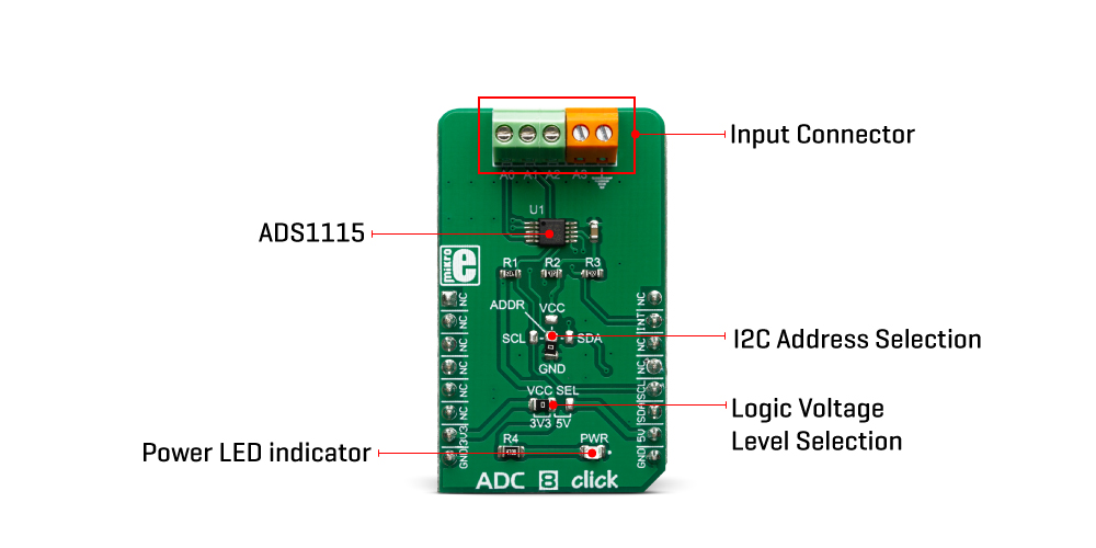
The main component of ADC 8 click is the ADS1115 IC, an ultra-small, low-power, high-precision, 16-bit A/D converter, from Analog Devices. It is a delta-sigma converter with an integrated high-precision voltage reference, which can be programmed in several different steps. The maximum data rate of this ADC is 860 SPS, however, it features an excellent signal-to-noise ratio (SNR). The ADS1115 has two differential or four single-ended inputs. The internal multiplexer is used to select the active input. The input pins are routed to two input terminals on the edge of the Click board™, allowing it to be easily interfaced with the analog signal source.

Besides power supply pins and I2C interface pins, the ADS1115 has an additional ALERT/RDY pin used to signal that there is a conversion data available on the output register. This pin can also be set to output an overvoltage event. An internal comparator module can detect if the input signal exceeds the voltage reference level and report the overvoltage event at the ALERT/RDY pin. This pin is routed to the mikroBUS™ INT pin. Both I2C pins along with the ALERT/RDY pin, are pulled to a HIGH logic level by the pull-up resistors.
The conversion output is available over the I2C interface, in 16-bit two’s complement LSB/MSB format. A positive input signal can have values in the range from 0x0001 to 0x7FFF, while the negative input signal can have values in the range from 0x0000 to 0x8000. The slave I2C address of the device can be selected by moving the SMD jumper labeled as ADDR. It allows four different I2C addresses to be selected and thus, up to four different ADC 8 clicks can be used on a single I2C bus.
Signal to Noise ratio (SNR) depends on two factors: the reference voltage and the output data rate. Delta-sigma ADCs are based on the oversampling principle: the input signal is sampled at a higher frequency and it is subsequently filtered and decimated, until the output value is obtained, at the requested output data rate. The ratio between the high sampling frequency (modulator) and the output data rate is called oversampling ratio (OSR). By increasing the OSR, less noise appears at the output, since more values are included in the averaging process.
As already mentioned, the ADS1115 IC cannot use an external voltage reference. However, it has a high-precision internal reference with low drift over temperature. It can be selected from several available values: ±0.256, ±0.512, ±1.024, ±2.048V, ±4.096, and ±6.144. Note, however, that the input signal should not be greater than VCC + 0.3V. In other words, it is not possible to use the 4.096V if the power supply source is 3.3V. ADC 8 click is equipped with the SMD jumper labeled as VCC SEL, which allows selection between 3.3V and 5V.
Specifications
| Type | ADC |
| Applications | It is well suited for portable instrumentation applications, battery voltage, and current monitoring, analog sensor output conversion, etc. |
| On-board modules | ADS1115 IC, an ultra-small, low-power, high-precision, 16-bit A/D converter, from Analog Devices. |
| Key Features | Analog to digital conversion from 4 single-ended channels or 2 differential input channels, sampling resolution of 16 bits over the I2C interface, programmable high-precision internal reference… |
| Interface | I2C |
| Input Voltage | 3.3V or 5V |
| Click board size | M (42.9 x 25.4 mm) |
Pinout Diagram
This table shows how the pinout on ADC 8 Click corresponds to the pinout on the mikroBUS™ socket (the latter shown in the two middle columns).
Onboard Settings And Indicators
| Label | Name | Default | Description |
|---|---|---|---|
| LD1 | PWR | - | Power LED indicator |
| JP1 | VREF SEL | Left | Power supply voltage selection, left position 3.3V, right 5V |
| JP2, JP3 | ADDR | Down | Slave I2C Address Selection |
Software Support
We provide a library for the ADC 8 Click on our LibStock page, as well as a demo application (example), developed using MikroElektronika compilers. The demo can run on all the main MikroElektronika development boards.
Library Description
The library contains functions for the complete communication of the MCU with click. The user can use functions to read the ADC values and voltage on the channel. The library also offers functions for writting data into the register and reading data from the register, as well as the configuration of the device for successful measurement.
Key functions:
float adc8_getVoltage(uint8_t channel)- Read Voltage in mVuint16_t adc8_getADCValue(uint8_t channel)- Get ADC value reads from the channelvoid adc8_deviceConfig(uint16_t cfg)- Device configuration for measurement
Examples description
The application is composed of the three sections :
- System Initialization - Initializes I2C module and sets INT pin as INPUT
- Application Initialization - Initialization driver init and configuration device for measurement.
- Application Task - Reads voltage from each channel one by one and the voltage difference between specified channels
Note: On the input channel AIN0,AIN1,AIN2 and AIN3 sets maximum voltage GND - 0.3V < VIN > VDD + 0.3V.
void applicationTask()
{
    // Single channel
    vSingle_CH0 = adc8_getVoltage(_ADC8_SINGLE_CHANNEL_0);
    vSingle_CH1 = adc8_getVoltage(_ADC8_SINGLE_CHANNEL_1);
    vSingle_CH2 = adc8_getVoltage(_ADC8_SINGLE_CHANNEL_2);
    vSingle_CH3 = adc8_getVoltage(_ADC8_SINGLE_CHANNEL_3);

    mikrobus_logWrite("______________________________________________", _LOG_LINE);
    mikrobus_logWrite(" Channel |  CH 0  |  CH 1  |  CH 2  |  CH 3  |", _LOG_LINE);
    mikrobus_logWrite(" Single  |", _LOG_TEXT);

    IntToStr(vSingle_CH0, demoText);
    mikrobus_logWrite(demoText, _LOG_TEXT);
    mikrobus_logWrite("  |", _LOG_TEXT);

    IntToStr(vSingle_CH1, demoText);
    mikrobus_logWrite(demoText, _LOG_TEXT);
    mikrobus_logWrite("  |", _LOG_TEXT);

    IntToStr(vSingle_CH2, demoText);
    mikrobus_logWrite(demoText, _LOG_TEXT);
    mikrobus_logWrite("  |", _LOG_TEXT);

    IntToStr(vSingle_CH3, demoText);
    mikrobus_logWrite(demoText, _LOG_TEXT);
    mikrobus_logWrite("  |", _LOG_LINE);

    // Diff channel
    vDiff_CH01 = adc8_getVoltage(_ADC8_DIFF_CHANNEL_0_1);
    vDiff_CH03 = adc8_getVoltage(_ADC8_DIFF_CHANNEL_0_3);
    vDiff_CH13 = adc8_getVoltage(_ADC8_DIFF_CHANNEL_1_3);
    vDiff_CH23 = adc8_getVoltage(_ADC8_DIFF_CHANNEL_2_3);

    mikrobus_logWrite("______________________________________________", _LOG_LINE);
    mikrobus_logWrite(" Channel | CH 0-1 | CH 0-3 | CH 1-3 | CH 2-3 |", _LOG_LINE);
    mikrobus_logWrite("  Diff   |", _LOG_TEXT);

    IntToStr(vDiff_CH01, demoText);
    mikrobus_logWrite(demoText, _LOG_TEXT);
    mikrobus_logWrite("  |", _LOG_TEXT);

    IntToStr(vDiff_CH03, demoText);
    mikrobus_logWrite(demoText, _LOG_TEXT);
    mikrobus_logWrite("  |", _LOG_TEXT);

    IntToStr(vDiff_CH13, demoText);
    mikrobus_logWrite(demoText, _LOG_TEXT);
    mikrobus_logWrite("  |", _LOG_TEXT);

    IntToStr(vDiff_CH23, demoText);
    mikrobus_logWrite(demoText, _LOG_TEXT);
    mikrobus_logWrite("  |", _LOG_LINE);

    mikrobus_logWrite("|--------------------------------------------|", _LOG_LINE);
    Delay_1sec();
}
The full application code, and ready to use projects can be found on our LibStock page.
Other mikroE Libraries used in the example:
I2CConversions
Additional notes and informations
Depending on the development board you are using, you may need USB UART click, USB UART 2 click or RS232 click to connect to your PC, for development systems with no UART to USB interface available on the board. The terminal available in all MikroElektronika compilers, or any other terminal application of your choice, can be used to read the message.
MIKROSDK
This click board is supported with mikroSDK - MikroElektronika Software Development Kit. To ensure proper operation of mikroSDK compliant click board demo applications, mikroSDK should be downloaded from the LibStock and installed for the compiler you are using.
For more information about mikroSDK, visit the official page.
Downloads
Enter the code in the box below:


